Jun 06 2019

A telegram about the datagram: Short history of OSI

Short history of OSI

This post is based on the article  “The Internet that wasn’t” by  Andrew L. Russell [Russell13] published in IEEE Spectrum in 2013. The author is Assistant Professor of History at the Stevens Institute of Technology, N.J., USA and he wrote a prior article in 2006 about OSI history [Russell06] and felt that it has to be updated in 2013. The aim of this post is just to present a (telegraphic) summary, so if you are really interested in the subject I recommend you to read the original articles.

Prof. Russell was enticed to update the information after receiveing several emails from OSI (Open System Interconnection standard) veterans complaining about the way he pictured OSI in [Russell06]. He wrote a book in 2014 telling the story of OSI [Russell14].

Introduction

By the end of the 1970s a group of computer industry representatives from France, U.K. and U.S.A. started developing a computer network standard. This standard was called OSI: Open Systems Interconnection. Their goal was to enable global exchange of information. In 1980 thousands of engineers were involved in this project and OSI seemed a reality. However, in 1990 OSI was stalled and TCP/IP was adopted as the standard for world wide computer communications.

This story goes back to the 1960s.

1960

In this era computer communications was a hot research topic. Packet switching arises, being Paul Baran (Rand Corporation, USA), and Donald Davies (National Physics Lab, UK) the leaders supporting this technique. The idea is that data is decomposed in discrete blocks (packets) that are routed separately and the receiver reassembles the packet to obtain the original message. This was more efficient than circuit switching, that was based in predetermining the whole path between transmitter and receiver.

In 1969, researchers from DARPA (Defense’s Advanced Research Projects Agency) created the first packet-switched network: ARPANET.  IBM and European telephone monopolies started similar projects. IBM mimicked circuit switching with the so-called virtual circuits, reusing established technology. Thus, constraining the development packet switching.

1970

In 1972 the International Network Working Group (INWG) was created to standardize packet switching. The parties were USA, UK and France. Some active members were Vint Cerf (USA, first chairman of INWG) and Louis Pouzin (France).

Pouzin – leader of Cyclades, the French packet switching project – proposed the idea of the datagram: packets are sent without creating a connection. INWG supported the datagram.

In 1974 Cerf and Robert Kahn (DARPA) published the basis of the Internet elaborating on the ideas of Pouzin [Cerf74].

In 1975 the network protocol was submitting to CCITT (Consultative Committee for International Telegraphy and Telephony), but it was rejected.  INWG blamed circuit switching supporters for the negative response. In this very year (1975)  Cerf leaves for DARPA and there he works with Bob Kahn.

In 1977 UK proposed to ISO (International Standardization Organization) the creation of a standard for packet switching. This idea was supported by France and USA. The goal was to interconnect any kind of computer. This standard would supposse to break the monopoly from big companies. That was the creation of the “Open Systems Interconnection”: OSI.

Charles Backman (database expert) was the committee chairman. He proposed a model based on IBM Systems Network Architecture. However, OSI supported heterogeneity, and this was most welcomed by many companies with many different computing systems: General Motors.

Pouzin abandoned French packet switching network after struggling to get funding from the French government in 1978.

OSI model was based on layers, which enabled modularity, thus, there were different committees and working groups for each layer. In order to become an international standard it was necessary to fulfill with the following ISO’s 4-step process:

  1.  Working draft
  2.  Draft proposed international standard
  3. Draft international standard
  4. International standard

The first plenary meeting was held on the 28th of Feb. 1978.  10 countries and observers from international organizations attended. IBM managed to convinced OSI to include many of their business interests.
OSI forged and alliance with CCITT, so… datagram vs virtual circuits, again! Both points of views were included in OSI’s complexity. Chronicle of a death foretold: lots of layers, lots of parties involved, datagram, virtual circuits…

1980

OSI reference model is published as an international standard in 1984. There were individual standards for:

  •  transport protocols
  • electronic mail
  • network management
  • etc.


Meanwhile, USA developed TCP/IP and it was adopted as the Internet Protocol in 1983. Odd enough, the TCP/IP group joined OSI in 1985 and they wanted to apply the layers of OSI to the TCP/IP model. Also they wanted to have all USA computers complying with OSI by 1990.

In 1989 OSI is still under development and there were many concerns from OSI people:

  • Lots of money invested from companies, USA and European Community.
  • Internet looked very attractive and it was already working (what was the point of OSI then?).


1990

In the mid-1990 it was clear that OSI was not happening. The main problems were:

  • Too many interested parties
  • Too much bureaucracy
  • Too complex


Internet was adopted because:

  • Internet standards were free, while OSI standards were not
  • It was up and running (in USA)
  • It also promoted openness


OSI was seen as an incomprehensible stardard but it did have some good points:

  • It has a better architecture
  • It was more complete


Proof of that is that in 1992 the routing layer of TCP/IP was modified according to OSI ideas. Nowadays, OSI is still being taught at the universities along with TCP/IP.

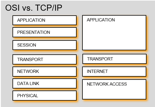
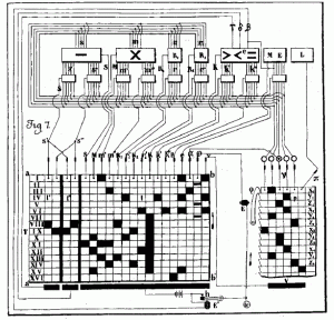
The complexity difference between the OSI and TCP/IP can be clearly seen in the following figure:

Final remarks

OSI was interested, but it became a monster difficult to tame. Finally, the practical and thorough approach of TCP/IP managed to make the Internet a reality. Summarizing: “OSI is a beautiful dream, TCP/IP is living it” [Russell13].

I would like to finish this post giving a thought to Pouzin’s French Packet Switching project from the early 70s. In a parallel universe the Internet is French 😉 .

Bibliography

[Russell13] “The Internet that wasn’t”, Andrew L. Russell, IEEE Spectrum, 2013

[Russell06] “Open Systems Interconnections (OSI) and the Internet”, Andrew L. Russell, IEEE Annals of the History of Computing, 2006

[Russell14] “Open Standards and the Digital Age: History, Ideology and Networks”,  Andrew L. Russell,, Cambridge University Press, 2014

[Cerf74] “A Protocol for Packet Network Intercommunication”, V. Cerf, R. Kahn, IEEE Transactions on Communications, 1974

Apr 30 2019

About timing diagrams of Moore finite state machines

About timing diagrams of Moore finite state machines

Finite state machines (FSMs) in the context of digital electronics are circuits able to generate a sequence of signals (i.e. outputs) that react according to the current state of the system and the values of input signals. The goal of this post is to explain how to draw timing diagrams of Moore finite state machines, motivated by the fact that after several years teaching Digital Electronics this issue seems to be quite difficult to understand for the students. I assume that the reader knows the basics of combinational logic and sequential logic, so I will dedicate just brief comments abobut the basis of state machines. So if you know a lot about timing diagrams of FSMs this might be not very challenging for you.

Let’s start.


Finite state machines

FSMs are used to generate a sequence of control signals that react to the value of inputs. The sequence is synchronous with a periodic clock signal. They consist of:

  • State register that
    • Store the current state
    • Load the next state at the clock edge
  • Combinational logic that
    • Computes the next state (next state logic)
    • Computes the outputs (output logic)

The following figure displays the symbols used for the state register, the next state logic and the output logic blocks.

Main parts of FSM

The next state is determined by the current state and the inputs. While the output is commonly generated using two approaches:

  • Moore FSM: the outputs depend only on the current state (Edward F. Moore, 1956 – not to be confused with Gordon Moore ) [Moore1956]
  • Mealy FSM: outputs depend on the current state and the inputs (George H. Mealy, 1955) [Mealy1955]

Here, we focused on Moore state machines. For a complete description of FSMs (and Digital Electronics in general) I recommend the book [Harris2012].

In the next figure, a block diagram of a Moore FSM is depicted.

Moore FSM

I will explain briefly the behaviour.

  • The RESET signal resets the current state S to an initial state (i.e. S0).
  • The state S is used in conjunction with the inputs to generate the next state S’. The “next state logic” block is implemented with logic gates so any changes in the inputs or the state will produce a change in S’. This change is not immediate, since the changes must propagate through the logics gates.
  • Regarding the state register, it can be seen that the data is stored with the rising edge of the clock signal (e.g. CLK goes from 0 to 1). This, given that the reset signal is not active, the next state S’ will become the current state S when a rising clock edge occurs. We assume here that S=S’ immediately assuming that the propagation delay of the register (i.e. tpcq) is zero seconds. Again, a change in S might produce a change in S’ (after the propagation delay of the next state logic).
  • The outputs depend on the current state S, so everytime the state changes the output might change. Since the output block is composed of logic there will be a propagation delay, so the outputs are not updated immediately after the state changes.


FSM example

As an example, we are going to design a FSM that reads a sequence of zeros and ones to detect the pattern “101”. Note that the last “1” of one pattern can be the beggining of a new pattern. This is better seen graphically:


An example of a binary sequence

The first two patterns are overlapped. The FSM must produce a one everytime the pattern is found and a zero otherwise.

The input to the systems is the sequence (A). Also we can consider the clock CLK and the RESET as signal inputs. There will be only one output signal that we will call Y.

Black box of FSM

The behaviour of a FSM is defined by a state transition diagram. The transition diagram for this example is:

State transition diagram of example

Note that there are 4 states represented with circles. Each circle includes the name of the state (i.e. S0, S1,…) and the value of the output Y. The initial state is S0 and it will be the current state if the RESET signal is active (this is represented in the diagram with the black arrow). The arcs represent the transitions from one state to another and the condition that must be fulfilled to change the state is written close to the arc.

Relating the state transition diagram with the Moore FSM block diagram, we can say that the states are associate with signal S; the arcs are associated with signal S’, and therefore, with the next state logic; and the outputs and the output logic with the output values displayed in each state circle.

Timing diagrams: steps to follow

Reset

We assume that the reset signal is active high, that is:

  • If RESET=1 then the output of the register is all zeros, so S=S0, being S0 the initial state. In this example we assume that this happens immediately with no delay.
  • IF RESET=0 the value of the output of the register will be kept until a clock edge (transition from 0 to 1) occurs, and the value of S will be replaced by S’ for a whole clock period.

RESET step

Clock edge (assuming that RESET=0)

We assume that the register react to rising clock edges (edge from 0 to 1) :

  • S=S’ just after the clock edge (there will be a minor delay due to the propagation time of the registers that we will consider negligible – tpcq=0).


Clock edge step


Outputs after the clock edge (assuming that RESET=0)

If S changed, then the outputs might change depending on the current state (see state transition diagram)

There will be a delay due to the propagation delay of the combinational logic of the “output logic” block.

Output step


Next state

If S changed then the next state S’ might change depending on the values of S and the inputs (see state transition diagram). Also if the inputs change this might produce an update in the value of S’.

The change will have a delay due to the propagation delay of the combinational logic of the “next state logic” block.

Next state step

Drawing the timing diagram

In order to draw the timing diagram we require to specify the values of:

  • The clock and the reset signal
  • The inputs

With that information and following the previous steps it will be possible to obtain the values of the outputs

  • It is necessary to obtain the value of S, which depends on the value of S’
  • S and S’ must be part of the diagram

Since the outputs are directly related to S we can leave them to the end and focus on S and S’

Step 1

To start, we draw the values of the clock (peridodic signal), the reset and the inputs. It is the task of the designed to select a sensible combination for these signals. Note that the values of S’ and S will be required in order to obtain the values of the outputs.

It is important to have close the transition diagram as well as the general Moore FSM block diagram to be able to fill in the values of S’, S and the outputs.

Step 1

Step 2

The initial values of S’ and S are unkown until there is a reset.

Step 2

Step 3

In this step we see to the effect of the reset signal. Note that now S=S0 (see transition diagram) and the value of S won’t change for a while (in fact, it might change only after RESET is inactive and if there is a rising clock edge).

Step 3

Step 4

Now let’s see the effect that updating S has on S’. We have to consider the values of S and the inputs. Note that S is stable for a while but S’ changes several times because the inputs change.

Step 4

Step 5

Now we focus on the moment when REST goes to zero. As aforementioned, the current state S does not change until there is a clock edge, so we extend the value of S (we could have done so in step 3 for sure).

Step 5

Step 6

We can see that the inputs change before the clock edge. Since we know the value of S it is possible to update S’. We stop jsut before the rising edge because it is then when the current state S will be updated and this might affect the value of S’.

Step 6

Step 7

At the rising clock edge S=S’=S1. This value will be stable for the whole clock period.

Step 7

Step 8

Now, after the clock edge, we can update S’. This time we update the whole clock period. The first change (S’=S1) is due to the change of S to S1, and the second change (S’=S10) is due to a change in the input. Check the transition diagram to see that this next state values are correct. Also note that only the last change just before the rising clock edge will be registered.

You should notice that once we are alternating the following:

  1. Update S with the rising clock edge.
  2. Update S’ with any change in the inputs or in S

Step 8

Step 9

Since the process is quite repetitive we start updateing more than one signal in the following steps.  Here we are updating, first S, and then S’ and the figure shows the result.

Step 9

Step 10

Again, we have updated, first S and then, S’. Note that S’ changes three times in the clock period. We are getting close to a new reset, so this should get more interesting (if that is even possible… 🙂 )

Step 10

Step 11

In this step we are updating S and S’ just before the RESET signal turn 1 again. S was updated just after the clock edge and in this case S’ does not change due to the value of the inputs (check transition diagram).

Step 11

Step 12

The RESET signal is resetting the state to S0. This change is permanent until the next valid rising clock edge, that is the next rising clock edge after RESET goes back to 0. Let’s draw all the values for S and S’ in the next step.

Step 12

Step 13

Step 13

Step 14

And the last step is filling in the outputs. Since there is a valus of the output per state it is straightforward.

Step 14


That’s all. I hope that this post is useful for students of Digital Electronics and for anyone in general (?). Dream with finite state machines, I will for sure.

This time the post was quite academic, but I will be back soon with something different. Some FPGAs could be good.


References

[Moore1956] E. F. Moore “Gedanken-experiments on sequential machines. Automata studies”, J. Annals of Mathematics studies, no. 34, 1956.

[Mealy1955] G. H. Mealy, “A method for synthesizing sequential circuits,” The Bell System Technical Journal, 1955.

[Harris2012] D. Harris, S. Harris, “Digital Design and Computer Architecture”, Morgan Kaufman, 2012.

Mar 30 2019

Fast binary conversion – Part II

[Fast binary conversion – part I]

In this post we continue talking about fast binary conversion, this time focusing on signed numbers, in particular two’s complement (2C) numbers .  We introduced binary in a previous post (Sinistar), and two’s complement was only briefly tackled:

” In 2C’s representation, the most significant bit (the one most to the left) is the sign bit. Positive numbers would have this bit to zero and negative numbers to one. The value of the number can be obtained like this: valor = -b_{N-1}\cdot 2^{N-1} + {\sum_{i=0}^{N-2} b_i\cdot 2^i} = -b_{N-1}2^{N-1}+b_{N-2}2^{N-2}+\ldots +b_{1}2^{1}+b_{0}2^{0}.

So, number 3 would be represented with 8 bits as 00000011 and number -3 as 11111101. Do the maths to check that it fits. An interesting property of 2C numbers is that we can add them no matter their sign: the results will be positive of negative directly, and it will be correct (given that the result can be represented with the available bits). … you can easily check that if we add 3 and -3 in 2C the result is zero (00000011+11111101 = 100000000, dicarding the ninth bit). Thus, substracting one unit to a number is the same as adding -1, than in 2C binary turns out to be the number 11111111 … “

So let’s see if we can find ways to read 2C binary numbers quickcly.

Positive numbers

Positive numbers are those with a zero in the most significant bit (MSB) zero. So the negative most significant weight is multiplied by zero leading to a positive number. For instance, the 2C binary number 011 is 3, since 011_2=(-2^2)\times 0 + 2^1\times 1 + 2^0\times 1 = 3_{10}. Therefore if the MSB is zero, numbers are positive and we can apply the rules from part I.

So from now on we will stick to negative numbers.

All ones

An N-bit numbers with N ones are always equal to -1_{10}. The reasoning is straightforward:

111 \cdots 111_{2}=1000 \cdots 000_2+011 \cdots 111_2=(-2^{N-1})+(2^{N-1}-1)=-1_{10}

Here we have applied the consecutive ones rules to the second term of the addition. So:

1_2=-1_{10}


11_2=-1_{10}


111_2=-1_{10}

1111111111_2=-1_{10}

Etc.

More ones than zeros (for negative numbers) and 2C numbers in general

A number with more ones than zeros can be seen as a number with all ones with some ones substracted. For instance:

111101_2=111111_2-000010_2=-1_{10}-2_{10}=-3_{10} 1111010111_2=1111111111_2-0000101000_2 = -1_{10}-40_{10} = -41_{10}

From the example, it is simple to infer that a way to read a negative 2C number is to invert the number (flip zeros and ones), add one, and then apply a negative sign. So a negative number B can be converted to decimal performing the operation -(\bar{B}+1)=-\bar{B}-1. For instance, number 111101_2=-000010_2-1 = -2-1=-3. So now, it is up to you to see a negative 2C number as a -1 lacking some ones in the positions where there are zeros, or as the result of -1 multiplied by the value of the inverted binary number. minus one.

More zeros than ones (for negative numbers)

If there are more zeros than ones you might as well simply add the weigths of the corresponding ones:

10000001_2= -2^7+1=-127


1000101_2= -2^6+4+1=-59


1000000000_2= -2^9=-512


Zeros to the right

As with unsigned numbers (and positive 2C numbers), the effect of having zeros to the right is equivalent to a multiplication of a power of two. For negative number we have:

10100_2=101_2\cdot 2^2=-3\cdot4=-12

1111111111000_2=1111111111_2\cdot 2^3=-1\cdot 8=-8_{10}

11110101110000_2=1111010111_2\cdot 2^4 = -41_{10}\cdot 16 = -656_{10}

100010100_2=1000101_2\cdot2^2= (-2^6+4+1)\cdot 4=-61\cdot 4 = 244_{10}

Etc.

Putting all together

Let’s try to find the best way to perform fast conversion to several 2C  numbers.

010100000101=1024+256+5=1285

10100000101=-6\cdot128+5=-768+5=-763

011110000=15\cdot16=240

11110000=-1\cdot16=-16

011110111000=(255-8)\cdot8=247\cdot8=1976

11110111000=-9\cdot8=-72

Etc.

With this post and in part I I think that we have learnt a few useful tricks that can be handy if a calculator is not available.  It remains open if we will be proficient at communicating with moisture vaporators. Please let me know.

Feb 24 2019

Fast binary conversion – Part I

Binary is the basis of digital systems and it is important to be fluent when it comes to obtain the decimal value of a binary number. In this post we will start dealing with fast binary to decimal conversion for numbers up to 16 bits. This will be handy if you work in the domain of embedded systems and digital design.

In a previous post, we introduced the basics of binary number systems. I will reuse some paragraphs here:

” The binary system is a base-2 positional numeral system. A base-B positional numeral system represents numbers with digits that can have values from 0 to B-1 (from 0 to 1 for binary; from 0 to 9 for decimal, etc.), and they are written one after the other. A digit is in a position i which in turn determines its weight. Assuming that the digit located to the right of the number has position 0 and that the digit located to the left of the number has position N-1 (because there are N digits), the weight of each digit is B^i. Given that an N-digit number with values b_i (b_i\in [0\ldots B-1] and i\in [0\ldots N-1]), its value can be computed as:
value = \sum_{i=0}^{N-1} b_i\cdot 2^i = b_{N-1}2^{N-1}+b_{N-2}2^{N-2}+\ldots +b_{1}2^{1}+b_{0}2^{0}.
For instance, the binary number 10011_2 has a decimal value of 1\cdot2^4+0\cdot2^3+0\cdot2^2+1\cdot2^1+1\cdot2^0=16+2+1=19_{10}. “

Learning by heart a few powers of two is useful in many ways. Firstly, it is necessary to do any mental conversion from binary to decimal. So do your homework and learn the powers of two from 2^0 to 2^{16}; that is: 1, 2, 4, 8, 16, 32, 64, 128, 256, 512, 1024, 2048, 4096, 8192, 16384, 32768 and 65536. Once you know these powers of two, it is easy to find out the minimum number of bits that we need to represent an integer number. For instance, if we know the upper closest power of two of a number x, this will lead us to the number of bits required to represent that number. Let’s say that we want to convert to binary number 240. The upper closest power of two is 256, which is 2^8, which tells us that 8 bits are required. Note, that if the number is exactly a power of two (i.e. x=256) then the number of bits has to be increased by 1. And knowing these powers of two will be also essential in performing fast binary to decimal conversions.

So now, let’s start with some “shortcuts”

Consecutive ones

Let’s talk now about something quite trivial. If we add 1 to number 999, we obtain 1000. So 999=1000-1, that is 999=10^3-1, so, the exponent of the power of ten matches the number of consecutive nines. We can generalized this so that a number in base B composed of a sequence of N consecutive digits is equal to (B^N-1)_B, and particularizing for binary (B=2) a sequence of N consecutive ones is equal to (2^N-1)_{10}. So now, assuming that we master the powers of two, we can easily calculate the decimal value of numbers such as:

    • 11111_2=2^5-1=32-1=31
    • 1111111111_2=2^{10}-1=1024-1=1023
    • Etc.

Zeros on the right

Adding a zero to the right of a number is equivalent to multiplying the number by the base. For instance, 560_{10}=56\times10110_2=11_2\times 2, etc. Thus, adding N zeros to the right of a binary number is equivalent to multiplying the number by 2^N . This could be useful sometimes:

10100_2=101_2\cdot 2^2=5\cdot4=20 (also, 16+4=20)

1111111111000_2=1111111111_2\cdot 2^3=(2^{10}-1)\cdot 8=1023\cdot8=8184

Etc.

More ones than zeros

If a binary number has just a few zeros you might as well consider the number as a sequence of consecutive ones that has a few ones missing. Thus, number 111111110111_2 can be seen as 111111111111_2-1000_2=(2^{12}-1)-2^3=4095_{10}-8_{10}=4087_{10}. Let’s see some examples:

10111101_2=(2^8-1)-2^7-2^1=255-66=189

111111111100_2=(2^{12}-1)-3=4092 (or, 1023\cdot4=4092)

Putting all together

Let’s try to find the best way to perform fast conversion to several numbers. I am assuming here that you master powers of two and that you easily recognize short binary numbers.

10100000101=1024+256+5=1285

10100000101=5\cdot 2^8 + 5=5\cdot 257 = 1285

11110000=15\cdot16=240

11110111000=(255-8)\cdot8=247\cdot8=1976

11110111000=2047-64-7=2040-71=1976

1000000000001=4096+1=4097

1000000001110=4096+(7\cdot2)=4096+14=4110

111101000=8\cdot(63-2)=8\cdot61=488

Etc.


Well, it is not rocket science, but surely it is useful. You will find many occasions when these tricks cannot be applied and you have to add all the weights corresponding to the ones to obtain the decimal values. Also, you can use a calculator 🙂 .

In this post we have covered unsigned numbers. The next post we’ll be about fast conversion of signed binary numbers: two’s complement numbers. Stay tune and soon you will master the binary language of moisture vaporators (Star Wars rules!) . See you soon!


Feb 01 2019

Torres Quevedo and the first computer

(originally published in Spanish in November 2018)

I am in the middle of intensive reading up on the inventions of Leonardo Torres Quevedo, and, even though is a bit early, I would like to share my findings, especially those related with the world of computing. Additionally, I am Spanish and I talk all the time about pioneers of Electronics and Computing born or that lived in U.S.A., Japan, etc., and I think that it is not a bad idea to look for the national heroes now and then. Not pretending to underestimate anyone, I believe that there is a clear americanization of the history of computing, so instead of letting the information to find you, one has to make a special effort to look for it.

I start this research due to my interest in a line of computation that the general public assummes wrongly: computer (digital systems) commit mathematical errors when performing calculations. The main problem is that the number of digits that a computer uses to store a number is finite, thus, not all numeric values can be represented correctly, and this leads to operations’ results with errors, which are propagated if these are used in other operations. It is at this point where I connect with Torres Quevedo, since I read somewhere that he was a pioneer proposing one of the arithmetic formats most used in modern computers at the beginning of the XX century.  “But that is another story and shall be told another time”, not so long.

This time I focus on something big: Torres Quevedo, a Spanish engineer, implemented the first computer in history.

Searching the IEEE and ACM databases yielded only a few articles: [Randell82][Yuste2005][Yuste2008]… I found a few Spanish books tackling this issue, some of them discontinued and others just passing through this issue or with incomplete information about it.  Randell deals with Torres Quevedo’s invention in his book “Origins of Digital Computers” (Springer, 1982),  but I did not have the oportunity to read it. There is a book about Torres Quevedo’s legacy by Alfonso Hernando González which is available online (check below). I have used the article by Randell [Randell82] as a starting point to traverse this path, along with the works of Hernando [Hernando1991] and the articles of Yuste et al [Yuste2005, Yuste2008].

Let’s start:

Leonardo Torres Quevedo was born on the 28 of December of 1852 in Santa Cruz (Cantabria, Spain). He studied Civil Engineering (Ingeniería de Caminos, Canales y Puertos) and his profesional carreer was full of achivements. He worked on different disciplines such as Aeronautics, Automatics, Telecommunications and Mechanics.  His inventions cover from analog computing machines, along with remote radio controlled systems, to the design and fabrication of semi-rigid planes that were used in the First World War. His “Spanish Aero Car” is still fully functional in Niagara’s Falls. He also was quite productive designing computing devices and automata.

File:El eminente sabio español Leonardo Torres Quevedo, de Franzen.jpg

The eminent Spanish wise man Leonardo Torres Quevedo (wikipedia)

His famous Chess Player, considered the first chess automaton,  was able to carry out the king and rooke endgame, playing – and winning—against a human opponent. It is possible to check its design in the publication Le Nature de 1914 [Vigneron1914].

File:El Ajedrecista de Leonardo Torres Quevedo 02.jpg

The Chess Player (el ajedrecista) by Leonardo Torres Quevedo (wikipedia)

He was keen on exploring the possibilities offered by electromechanic systems and to test the limits of machines. In his work Essays on Automatics (Ensayos sobre automática) [Torres1914] he elaborate on the work of Babbage, who was the first to propose the construction of machines able not only to perform mathematical operations, but also to execute a program.  The Analytical Engine was conceived to be entirely mechanical, was able to store data (as the registers in a CPU do), had arithmetic operators such as adders, multipliers and dividers (equivalent to the Arithmetic-Logic Unit (ALU) of a CPU) and its programs accounted for loops and decision making (conditional branches). Ada Lovelace stands out as the first programmer since she, inspired by Babagge work, wrote the first programs that could be run on a machine, even though neither her nor Babagge would seen the analytical engine built.  Eventually the machine was never built and Torres Quevedo used its design as a seed to carry out a functional electromechanical  implementation. In his eassy, he faced the design of machine able to perform the operation ax(y-z)2 given input values for the variables. The machine had the same blocks of Babagge’s machine, but adapted to the electromechanic technology of early 20th century: arithmetic block (i.e. ALU), temporal storing block (i.e. registers) and read-only program (i.e. ROM) that allowed conditional branches.

Automaton to compute ax(y-z)^2 (“Ensayos sobre automática” 1914)

After this intelectual effort, he built several prototypes and it is in 1920 when he presented in Paris the Arithmometer. This invention enabled writing the operation to be computed through a typewriter and the machine executed a program acording to the chosen operation. Inside, there was an only-read program that would control the arithmetic operators, the temporal memory, etc. In conclusion, a computer that was able to execute a program stored in a drum. In order to change the program it was necesary to build a new drum and insert it into the machine  [Hernando1991]. Quite close to punched card technology.

We must highlight that Torres Quevedo did not consider the use of massive storing memories (i.e. RAM), but only the storing of temporal values or final operations results – resembling the registers of a CPU. It is likely that the complexity of storing and addressing huge amounts of data was out of reach for the technology of the times.

In [Hernando1991] it is pointed out that the publication Essays on automatics (Ensayos sobre automática) is “one of the fundamental texts in the history of Informatics”. Hernando also prompts that Torres Quevedo brings out the importance of digital machines that allow controlling systems, while reacting to the environment conditions as well as to the very computed data. Clearly a visionary comment. Moreover, he proposes the creation of a specific study branch called Automatics. Had this been developed it would have been possible to research on several aspects of Electronics and Computer Science several decades before it actually happened. In addition, the inventor stresses that automata not only must focus on performing automatic mathematical calculations but they should also address any kind of problem, again foreseeing ideas that were developed several decades after by Turing, Von Neumann, etc. Hernando carried out this PhD Thesis on the work of Torres Quevedo and published on his blog a free copy of his book from 2000 about the same subject.

However, it seems that the impact of Torres Quevedo’s theories and inventions related to computing has been negligible, not affecting the course of Informatics due to the lack of difussion [Hernando1991]. Had his theories been spread, the history of Computing would have followed a different path, and the computer would have been created long before. The achivements of Leonardo Torres Quevedo are previous to those of Turing (who was born in 1912) and several decades previous to the computers of the 40s that set the foundations of modern Computing.

With this post, I simply tried to disseminate the relationship between Torres Quevedo and the history of Informatics, without being specific about the inner details of his inventions. I hope I have time to be able to analyze the designs of this awsome scientific and inventor so I can post about it in the future.

Related links

The Babbage Engine, Computer History Museum (accessed on 30/11/2018)

Biografía de Leonardo Torres Quevedo, ITEFI-CSIC (accessed on 30/11/2018)

Proceedings of the Symposium “Simposio Leonardo Torres Quevedo: su vida, su tiempo, su obra”, 1987, 1991 y 1995 (accessed on 30/11/2018)

Alfonso Hernando González’s blog (accessed on 30/11/2018)

References

[Randell1982] “From Analytical Engine to Electronic Digital Computer: The Contributions of Ledgate, Torres, and Bush”, Brian Randell, Annals of the History of Computing, IEEE, 1982

[Vigneron1914] «Les automates», H. vigneron Le Nature, 1914 (The Chessplayer)

[Torres1914] “Ensayos sobre Automática. Su definición. Extensión teórica”, L. Torres Quevedo, Revista de la Real Academia de las Ciencias, 1914 [PDF]

[Hernando1991] “Torres Quevedo como precursor de la informática moderna”, A. Hernando González, Proceedings of the Symposium “Simposio Leonardo Torres Quevedo: su vida, su tiempo, su obra”, 1991 [PDF]

[Yuste2005] “Scanning Our Past from Madrid: Leonardo Torres Quevedo”, A.P. Yuste, M.S. Palma, Proceedings IEEE, 2005

[Yuste2008] “Early Developments of Wireless Remote Control: The Telekino of Torres-Quevedo”, A.P. Yuste, Proceedings

Nov 06 2018

Sinistar: the arcade of the eternal youth

There is nothing like finding an arguably fun example to support any of the arid concepts populating the fields of digital electronics, computing and signal processing. Some time ago, I came across a fantastic video published by the IEEE Spectrum Magazine (Five Infamous Arcade-Game Glitches), devoted to programming mistakes (i.e. glitches) in arcade videogames: Asteroids (Atari), Donkey Kong (Nintendo), Sinistar (Williams Electronics), Ms. Pacman (Midway) and Centipede (Atari) .

Sinistar’s glitch got my attention, and it seemed handy to explain two’s complement arithmetic, which is essential in the digital systems domain. In this game, it was possible to go from having 1 life to enjoy 255 lives. And all due to a programming absent-mindedness and to the behavior of binary arithmetic. By the way, let me clarify that what goes next is quite simple, but fun.

First I will briefly explain some concepts about binary. If you think that this is too basic you can go straight to the heart of the issue clicking here.

Continue reading

Oct 08 2018

Total recall: “6502: igniting the digital revolution” (2017)

The 6502 was pure magic out of transistors. The creators of this microchip are truly digital heroes that achieved the unthinkable: creating a low-cost microprocessor in 1975 that shaped the electronic industry. This device was used in legendary machines, such as Atari VCS 2600, Apple II, Commodore 64, Nintendo Famicon, etc. An animated GIF is worth one thousand words:

(sometimes this GIF does not animate, try this)

In 2017 I gave two talks on this topic. First, in April 2017, I had the opportunity to pay homage to this wonderful tiny microprocessor by means of a presentation at the retrocomputing event RetroMadrid. Later, I extended a little bit the talk and gave it again as part of a research divulgation event organized by the government of Madrid (Semana de la Ciencia 2017, November 2017).  I deeply enjoyed the process of connecting the numerous dots that outline a fascinating and unique story. Also, I received lots of feedback from the audience that I very much appreciate. By the way, the end of the second talk is alternative… in many senses.

The contents of the talk cover:

  • Brief (and quite informal) review on digital circuits and integrated circuits
  • Chuck Peddle and Motorola: let’s compete with Intel!
  • Chuck Peddle and MOS Technology: Let’s build a low-cost microprocessor!
    • The 650x team
    • Design of the 650x chipset
    • Selling the micro
    • Motorola strikes back
  • 6502 and Commodore
  • 6502 and… Commodores, Atari, Apple, ARM, Nintendo, etc., etc.
  • The 6502 today
    • Books, microchips and kits
    • FPGAs
    • Visual6502
    • 6502 and neuroscience
  • The public goes wild


I must highlight that my talks were based on books and documents that later on I realized that some of them were not completely objective, so the story had some uncertainties that must be further investigated. I wish I have the time some day to do so. Since then, I try to be very careful with the sources I used and I always try to elaborate my own version of the story, clearly stating what is fact and what is an opinion (mine of somebody else’s). [I talked a little bit about that in my talk about the invention of the microprocessor]

Summarizing, no matter if you are sentimentally attached to Zilog, Motorola, Texas Instruments, etc., the story of the 6502 must be told, because this microprocessor is a key element to understand the creation of the PC and the birth of the videogame industry.

Some highlights

  • The microelectronic process was manual. They had to draw the different layers of the microchip by hand. This also happens with the Intel 4004.
  • A guy called Steve Wozniak bought a few chips from the first batch of 6502 to build the Apple I. This microprocessor made possible to build affordable computers.
  • Two of the three first best-seller personal computers that motivated IBM to enter the personal computer business had 6502 as brains: Apple II (6502), Commodore PET (6502) and Tandy TRS-80 (Z80).
  • The creation of the 6502 and the fact that a small company (Western Design Center) could design and produce microchip served as an inspiration to Acorn engineers to develop their own microprocessors and a few years later ARM was born.


Resources

6502.org: The 6502 microprocessor resource
The Visual 6502 project: Wanna see the transistor activity while executing assembly code? This is the place
Apple][ history website: The reference place to learn about the Apple ][
Commodore: a company on the edge: Amazing book about the first steps of Commodore Bussiness Machines into computing. The inception of the 6502 chip is beautifully described.

Talks (in Spanish)

  • El microprocesador 6502 y su impacto en la revolución digital (Spanish),  RetroMadrid 2017, [slides]
  • Historia del microprocesador 6502: semilla del PC y de la industria de los videojuegos (Spanish), Semana de la Ciencia 2017 [slides (with alternative ending 🙂 )]

Sep 05 2018

(RetroMadrid2018) 4- and 8-bit pioneers: the creation of the microprocessor [the talk I couldn’t give]

(Also available in Spanish. Use the language switch)
Please find a video (in Spanish) of a talk I planned to give in RetroMadrid 2018 (a Spanish event for retrocumputing), but that eventually I got sick and I could not attend. The talk covers the following points:

  • Review of my previous talk (history of 6502) in RetroMadrid 2017.
  • Origin of Intel 4004.
    • Highlight: The role of Japan in the creation of the first comercial microprocessor on 1 single chip.
    • Highlight: Two genius Dos genios en acción: Masatoshi Shima y Federico Faggin.
  • Was the Intel 4004 the first microprocessor? We will revisit the definition the definition of microprocessor and cover some microprocessor contemporary to 4004.
    • Highlight: I think that there were other microprocessor prior to Intel 4004 (my personal opinion).
  • Texas Instruments: a 45 years old secret.
  • Relationship of Intel with: Zilog, Motorola, MOS Technology, ARM, etc.
  • Yes, I like Star Wars 🙂


If you are in a hurry:

Some references:


Bitnami