
About timing diagrams of Moore finite state machines
Finite state machines (FSMs) in the context of digital electronics are circuits able to generate a sequence of signals (i.e. outputs) that react according to the current state of the system and the values of input signals. The goal of this post is to explain how to draw timing diagrams of Moore finite state machines, motivated by the fact that after several years teaching Digital Electronics this issue seems to be quite difficult to understand for the students. I assume that the reader knows the basics of combinational logic and sequential logic, so I will dedicate just brief comments abobut the basis of state machines. So if you know a lot about timing diagrams of FSMs this might be not very challenging for you.
Let’s start.
Finite state machines
FSMs are used to generate a sequence of control signals that react to the value of inputs. The sequence is synchronous with a periodic clock signal. They consist of:
- State register that
- Store the current state
- Load the next state at the clock edge
- Combinational logic that
- Computes the next state (next state logic)
- Computes the outputs (output logic)
- Computes the next state (next state logic)
The following figure displays the symbols used for the state register, the next state logic and the output logic blocks.
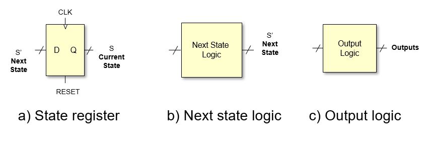
Main parts of FSM
The next state is determined by the current state and the inputs. While the output is commonly generated using two approaches:
- Moore FSM: the outputs depend only on the current state (Edward F. Moore, 1956 – not to be confused with Gordon Moore ) [Moore1956]
- Mealy FSM: outputs depend on the current state and the inputs (George H. Mealy, 1955) [Mealy1955]
Here, we focused on Moore state machines. For a complete description of FSMs (and Digital Electronics in general) I recommend the book [Harris2012].
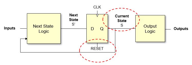
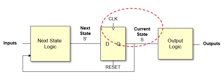
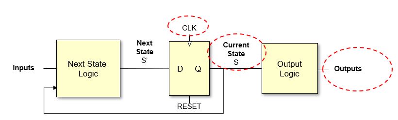
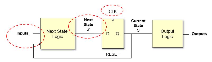
In the next figure, a block diagram of a Moore FSM is depicted.
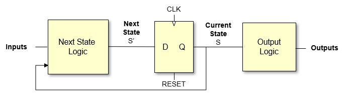
Moore FSM
I will explain briefly the behaviour.
- The RESET signal resets the current state S to an initial state (i.e. S0).
- The state S is used in conjunction with the inputs to generate the next state S’. The “next state logic” block is implemented with logic gates so any changes in the inputs or the state will produce a change in S’. This change is not immediate, since the changes must propagate through the logics gates.
- Regarding the state register, it can be seen that the data is stored with the rising edge of the clock signal (e.g. CLK goes from 0 to 1). This, given that the reset signal is not active, the next state S’ will become the current state S when a rising clock edge occurs. We assume here that S=S’ immediately assuming that the propagation delay of the register (i.e. tpcq) is zero seconds. Again, a change in S might produce a change in S’ (after the propagation delay of the next state logic).
- The outputs depend on the current state S, so everytime the state changes the output might change. Since the output block is composed of logic there will be a propagation delay, so the outputs are not updated immediately after the state changes.
FSM example
As an example, we are going to design a FSM that reads a sequence of zeros and ones to detect the pattern “101”. Note that the last “1” of one pattern can be the beggining of a new pattern. This is better seen graphically:
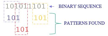
An example of a binary sequence
The first two patterns are overlapped. The FSM must produce a one everytime the pattern is found and a zero otherwise.
The input to the systems is the sequence (A). Also we can consider the clock CLK and the RESET as signal inputs. There will be only one output signal that we will call Y.
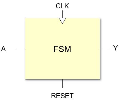
Black box of FSM
The behaviour of a FSM is defined by a state transition diagram. The transition diagram for this example is:
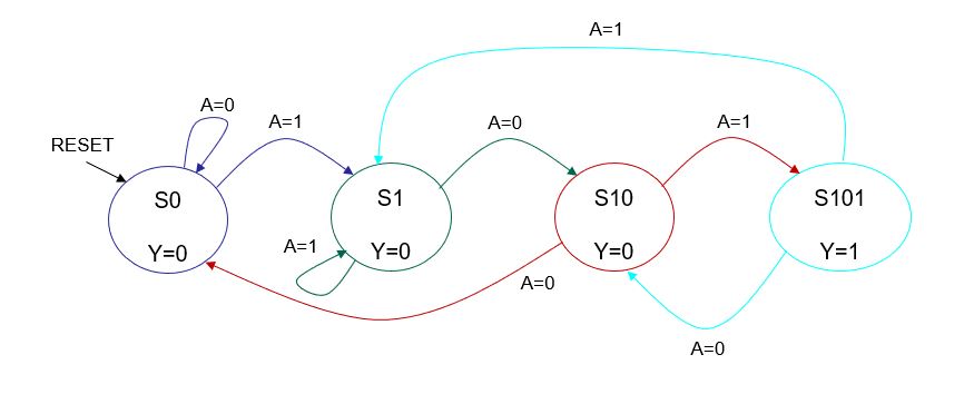
State transition diagram of example
Note that there are 4 states represented with circles. Each circle includes the name of the state (i.e. S0, S1,…) and the value of the output Y. The initial state is S0 and it will be the current state if the RESET signal is active (this is represented in the diagram with the black arrow). The arcs represent the transitions from one state to another and the condition that must be fulfilled to change the state is written close to the arc.
Relating the state transition diagram with the Moore FSM block diagram, we can say that the states are associate with signal S; the arcs are associated with signal S’, and therefore, with the next state logic; and the outputs and the output logic with the output values displayed in each state circle.
Timing diagrams: steps to follow
Reset
We assume that the reset signal is active high, that is:
- If RESET=1 then the output of the register is all zeros, so S=S0, being S0 the initial state. In this example we assume that this happens immediately with no delay.
- IF RESET=0 the value of the output of the register will be kept until a clock edge (transition from 0 to 1) occurs, and the value of S will be replaced by S’ for a whole clock period.
RESET step
Clock edge (assuming that RESET=0)
We assume that the register react to rising clock edges (edge from 0 to 1) :
- S=S’ just after the clock edge (there will be a minor delay due to the propagation time of the registers that we will consider negligible – tpcq=0).
Clock edge step
Outputs after the clock edge (assuming that RESET=0)
If S changed, then the outputs might change depending on the current state (see state transition diagram)
There will be a delay due to the propagation delay of the combinational logic of the “output logic” block.
Output step
Next state
If S changed then the next state S’ might change depending on the values of S and the inputs (see state transition diagram). Also if the inputs change this might produce an update in the value of S’.
The change will have a delay due to the propagation delay of the combinational logic of the “next state logic” block.
Next state step
Drawing the timing diagram
In order to draw the timing diagram we require to specify the values of:
- The clock and the reset signal
- The inputs
With that information and following the previous steps it will be possible to obtain the values of the outputs
- It is necessary to obtain the value of S, which depends on the value of S’
- S and S’ must be part of the diagram
Since the outputs are directly related to S we can leave them to the end and focus on S and S’
Step 1
To start, we draw the values of the clock (peridodic signal), the reset and the inputs. It is the task of the designed to select a sensible combination for these signals. Note that the values of S’ and S will be required in order to obtain the values of the outputs.
It is important to have close the transition diagram as well as the general Moore FSM block diagram to be able to fill in the values of S’, S and the outputs.
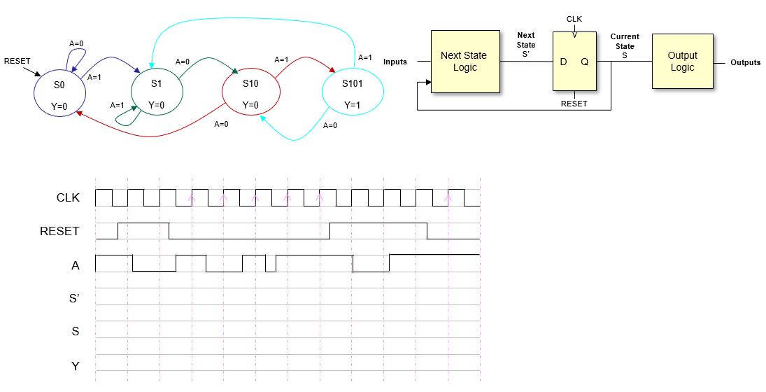
Step 1
Step 2
The initial values of S’ and S are unkown until there is a reset.
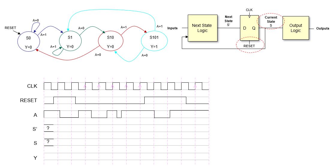
Step 2
Step 3
In this step we see to the effect of the reset signal. Note that now S=S0 (see transition diagram) and the value of S won’t change for a while (in fact, it might change only after RESET is inactive and if there is a rising clock edge).
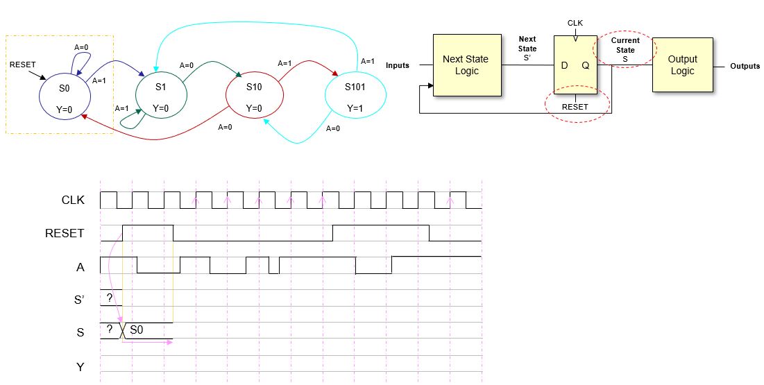
Step 3
Step 4
Now let’s see the effect that updating S has on S’. We have to consider the values of S and the inputs. Note that S is stable for a while but S’ changes several times because the inputs change.
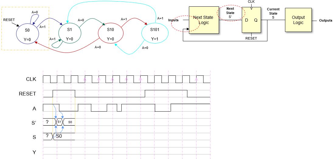
Step 4
Step 5
Now we focus on the moment when REST goes to zero. As aforementioned, the current state S does not change until there is a clock edge, so we extend the value of S (we could have done so in step 3 for sure).
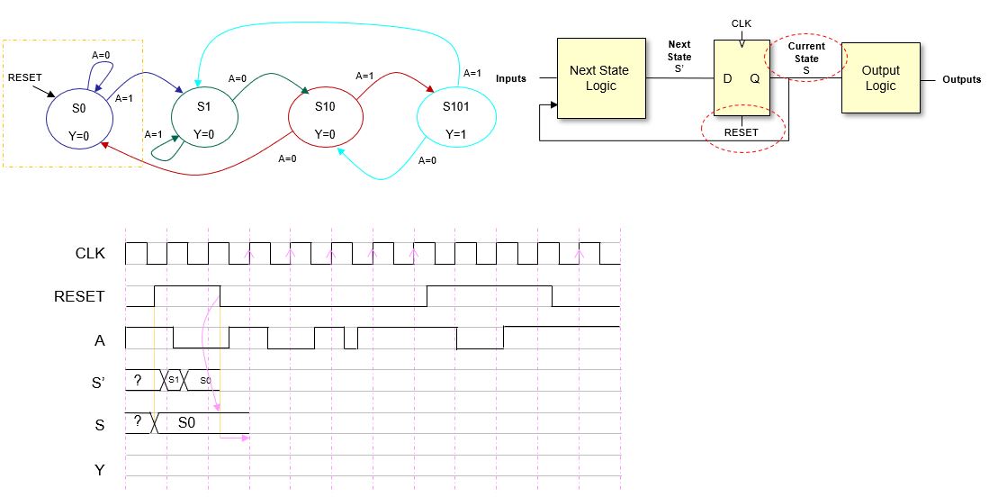
Step 5
Step 6
We can see that the inputs change before the clock edge. Since we know the value of S it is possible to update S’. We stop jsut before the rising edge because it is then when the current state S will be updated and this might affect the value of S’.
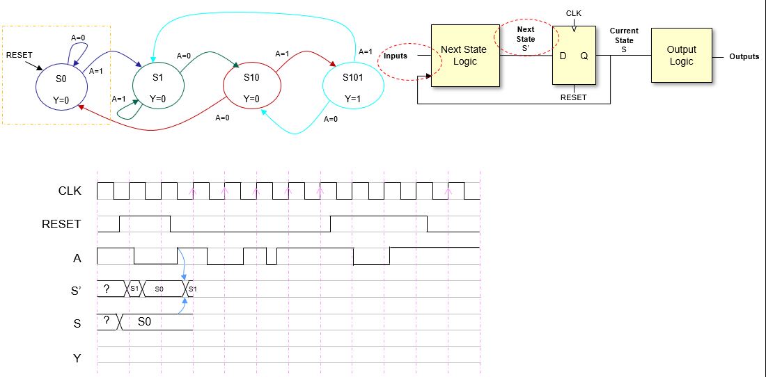
Step 6
Step 7
At the rising clock edge S=S’=S1. This value will be stable for the whole clock period.
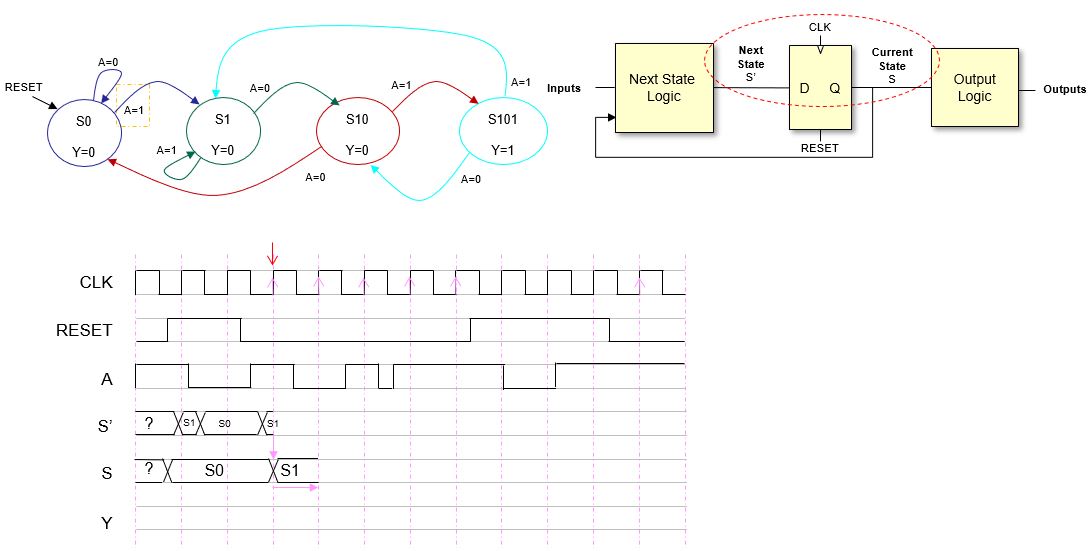
Step 7
Step 8
Now, after the clock edge, we can update S’. This time we update the whole clock period. The first change (S’=S1) is due to the change of S to S1, and the second change (S’=S10) is due to a change in the input. Check the transition diagram to see that this next state values are correct. Also note that only the last change just before the rising clock edge will be registered.
You should notice that once we are alternating the following:
- Update S with the rising clock edge.
- Update S’ with any change in the inputs or in S
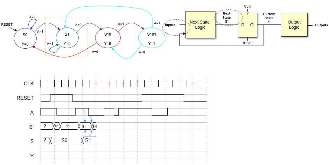
Step 8
Step 9
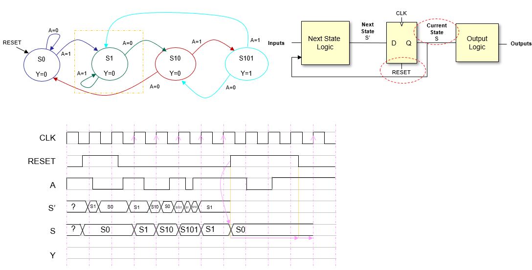
Since the process is quite repetitive we start updateing more than one signal in the following steps. Here we are updating, first S, and then S’ and the figure shows the result.
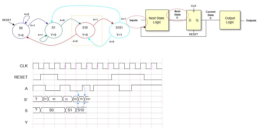
Step 9
Step 10
Again, we have updated, first S and then, S’. Note that S’ changes three times in the clock period. We are getting close to a new reset, so this should get more interesting (if that is even possible… 🙂 )
Step 10
Step 11
In this step we are updating S and S’ just before the RESET signal turn 1 again. S was updated just after the clock edge and in this case S’ does not change due to the value of the inputs (check transition diagram).
Step 11
Step 12
The RESET signal is resetting the state to S0. This change is permanent until the next valid rising clock edge, that is the next rising clock edge after RESET goes back to 0. Let’s draw all the values for S and S’ in the next step.
Step 12
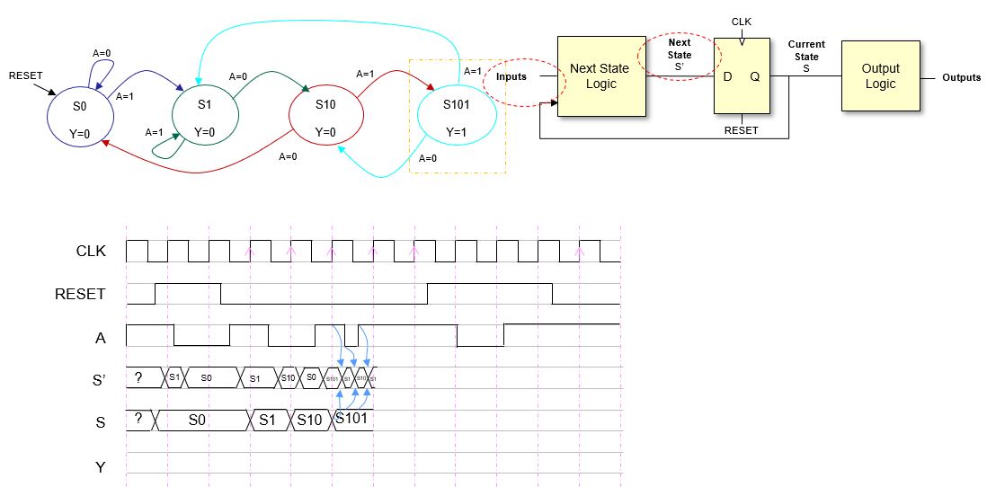
Step 13
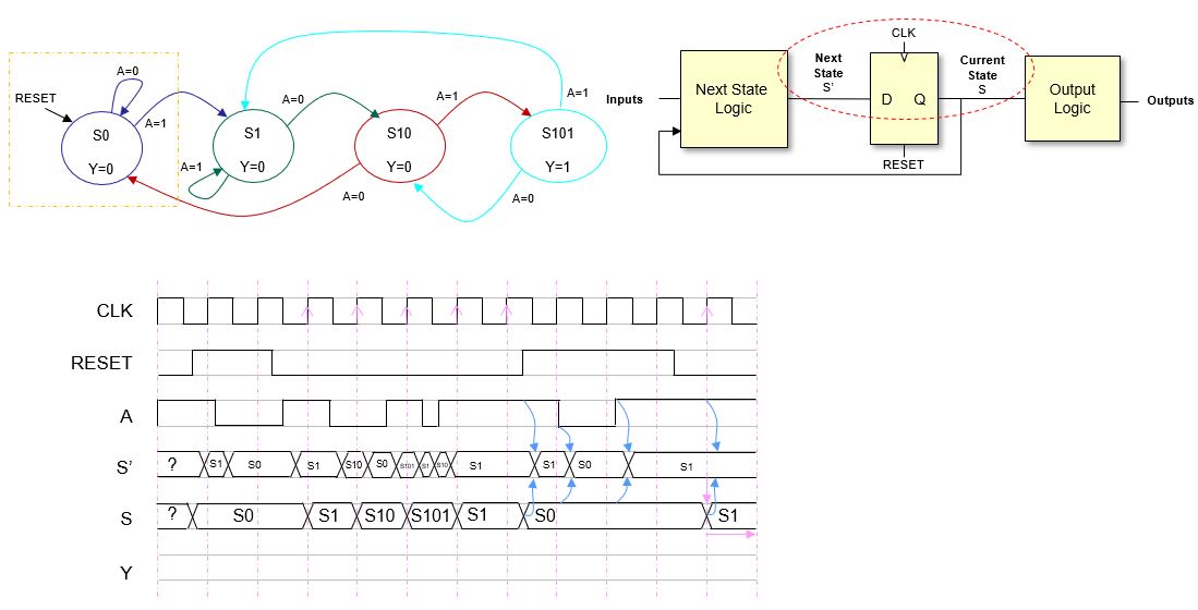
Step 13
Step 14
And the last step is filling in the outputs. Since there is a valus of the output per state it is straightforward.
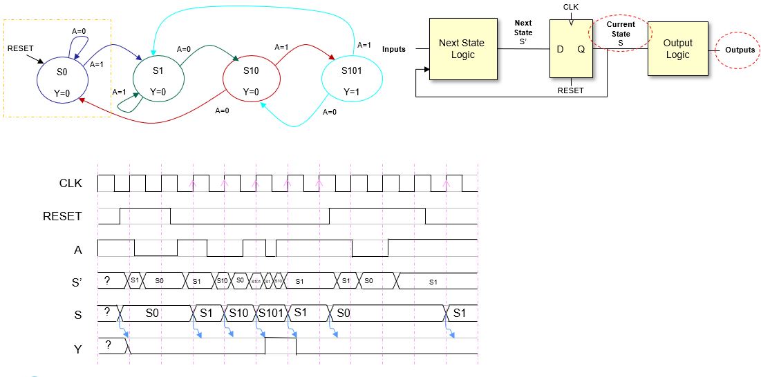
Step 14
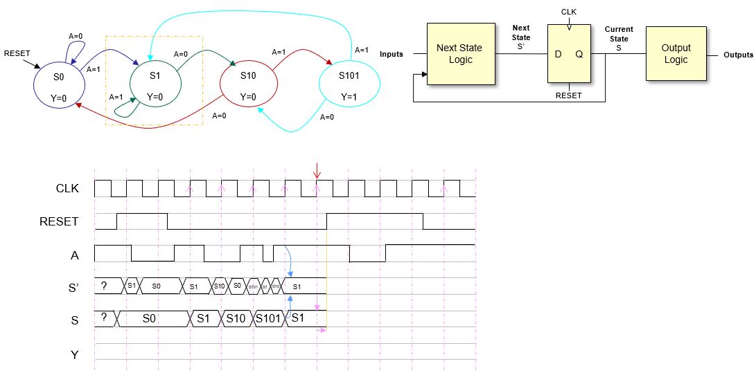
That’s all. I hope that this post is useful for students of Digital Electronics and for anyone in general (?). Dream with finite state machines, I will for sure.
This time the post was quite academic, but I will be back soon with something different. Some FPGAs could be good.
References
[Moore1956] E. F. Moore “Gedanken-experiments on sequential machines. Automata studies”, J. Annals of Mathematics studies, no. 34, 1956.
[Mealy1955] G. H. Mealy, “A method for synthesizing sequential circuits,” The Bell System Technical Journal, 1955.
[Harris2012] D. Harris, S. Harris, “Digital Design and Computer Architecture”, Morgan Kaufman, 2012.

